|
Introduction Transparent Conducting Oxide (TCO) films such as impurity-doped indium oxide, tin oxide, and zinc oxide systems have been widely used as transparent conductors for numerous optoelectronic applications, such as flat panel displays, touch screen devices, and photovoltaics [1 – 4]. Among these transparent conducting oxides, Indium Tin Oxide (ITO) is one of the most widely used because of its low resistivity and high optical transparency in the visible region. However, ITO is relatively expensive, brittle, unstable, and inflexible. Moreover, ITO transparency drops rapidly for wavelengths above 1,000 nm and requires a higher deposition temperature [5]. Indium Zinc Oxide (IZO) thin film has been reported to have an excellent conductivity, high optical transparency, and low deposition temperature [6-7]. Most importantly, the smooth surface and high etching rate of amorphous IZO thin films have been discussed [8]. A variety of techniques such as DC sputtering, RF sputtering, Pulsed Laser Deposition (PLD), Metal Organic Chemical Vapor Deposition (MOCVD), and spray pyrolysis have been used to deposit IZO films [9]. In this paper, we report on the factors controlling the surface morphology and electro-optical properties of ITO (10 wt. % ZnO + 90 wt. % In2O3) films deposited on microscope slide (Fisher Scientific Inc.) substrates with RF magnetron sputtering deposition. The electrical and optical properties of the IZO samples were examined as a function of the top IZO thickness, sputtering power, Argon gas flowing rate, and substrate tilt angle to optimize the conductivity and optical transparency of the IZO layer. In addition, surface morphology of the top IZO layer was evaluated by Scanning Electron Microscopy (SEM). Experiments An IZO (10 wt. % ZnO + 90 wt. % In2O3, 2.00” diameter, 0.125” thick, 99.99% pure) ceramic target (Kurt J. Lesker company) was placed at a distance of 50 mm from the main chamber of an AJA RF/DC magnetron sputtering system. The main chamber was equipped with a load-lock system and a diffusion pump which had a base pressure of 1.5 × 10⁻⁶ torr. The microscope slide substrates (1” x 1”) were cleaned in an ultrasonic bath of acetone at room temperature for 5 minutes, rinsed in deionized water in the ultrasonic bath for another 5 minutes, and then dried under N2 gas. The substrates were treated in Ultraviolet light for 15 minutes right beforethey were placed in the center of main chamber via the load-lock system from the side chamber of the sputtering system for being sputtered. The sputtering was carried out at room temperature and at a pressure between 8 × 10⁻³ and 2 × 10⁻⁴ torr in pure argon gas with varying sputtering parameters such as sputtering power, argon gas flow rate, and deposition thickness. Thickness of each deposited IZO layer was estimated by deposition rate from the sputtering system and was also measured by a thickness profilometer (Surfcorder ET-3000, Kosaka Laboratory Ltd.). Surface morphology of the top IZO layer was analyzed by a Scanning Electron Microscope (SEM). The optical transmittance was measured in the wavelength range of 300 – 1100 nm by UV/VIS/NIR spectrophotometer (Shimadzu Corp.) Results & Discussions Table 1 shows the sheet resistances of deposited IZO thin films varied with the RF sputtering powers applied with fixed 100 nm top IZO film thickness and 251 gas flowing rate. The lowest sheet resistance, 265 Ω/Sq, was found at 20 watts sputtering power. As the crystallinity of the IZO films increased with sputtering power, the grain size and surface roughness of the films increased, and electrical resistivity decreased. However, in this work, as the sputtering power increased beyond 25 W, electrical resistivity also increased. This might be due to a change in its phase or crystal structure as film deposition rate varied [10]. It also demonstrated a small influence of sputtering power on the optical transmittance at wavelength regions of 300 to 1100 nm.
Table 2 shows the sheet resistances of deposited IZO films as a function of argon gas flow rate with fixed 100 nm top IZO film thickness and 20 W sputtering power. The best electrical conductivity of the film was measured at an argon gas flow rate of 51. Increasing argon flow rates lead to increases in the thickness and the crack size on the films surface, which might have resulted in higher sheet resistance [11]. However, higher sheet resistance was also observed at very low argon flow rates. It might be due to decreasing the carrier concentration of the IZO films at low argon flow rates and decreasing the films growth rate. There were no observed significant differences for optical transmittance at wavelength regions of 300 to 1100 nm.
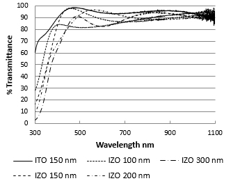
Table 3 shows that the sheet resistances of deposited IZO films decrease when the thickness increases with fixed 20 W sputtering power and 51 argon gas flow rate. The sheet resistance at 150 nm was 51 Ω/Sq which is close to ITO's at the same thickness (around 35 Ω/Sq). However, an increasing IZO deposited thickness resulted in a decrease of optical transmittance at ultraviolet wavelength regions of 300 to 400 nm, although a slight optical transmittance fluctuation was noticed at visible and near infrared regions of 400 to 1100 nm, as shown in Figure 1. The Figure also shows that ITO had a better optical transmittance performance in the ultraviolet region than IZO's.
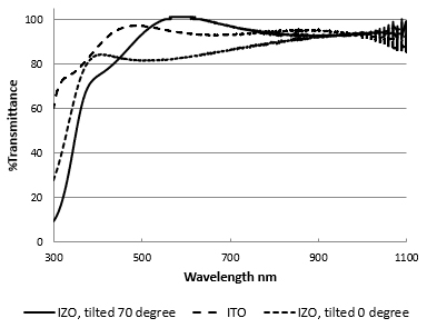
Table 4 shows the minimal sheet resistances 35 Ω/Sq at 700 tilt angle. The sputtering with tilt angles produced a columnar structure which reduced film stress induced by the defect variations in ZnO films [12], and thus at a 700 tilt angle sheet resistance decreases. Figure 2 shows the transmittance profile at the minimal sheet resistance did not make any noticeable changes compared with the profile with no tilt angles, a bit lower before 420 nm and a bit higher after 420 nm.
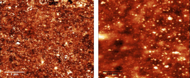
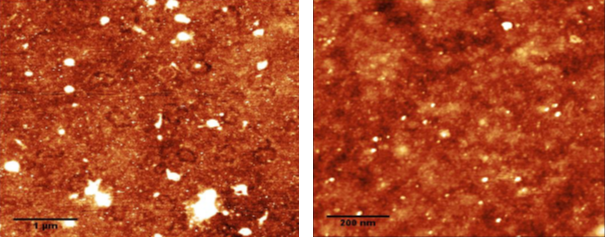
Figures 3 and 4 show AFM Images of surface topology of the top IZO layer with 100nm and 300 nm thickness under the processing condition of 51 argon flow rate and 20 watts sputtering power. In the case of the 300-nm-thick IZO layer (Figure 4), the AFM image is fairly smooth and featureless without defect crack pinholes, cracks, or protrusions on the surface of the top IZO layer. The RMS roughness of the area, excluding particulates, was Sq = 3.3 Å. In the case of the top IZO layer with a thickness of 100 nm (Figure 3), the AFM surface image had uniform defect crack pinholes and cracks. The RMS roughness of the area, excluding particulates, was Sq = 4.2 Å. The figures indicated that the surface of the top IZO layer got smoother with the increased thickness, and in the meanwhile, the sheet resistance would be reduced because the pinhole-like IZO layer was covered by the top IZO layer [5].
Conclusion In this work, amorphous Indium Zinc Oxide (IZO) thin films were deposited on the microscope slide substrates by using RF magnetron sputtering technique. We investigated the electrical and optical properties of these IZO thin films under different process conditions. We found the conductivity and optical transparency of the deposited IZO thin film very close to ITO's under the process condition at a 51 Argon flow rate, 20 W sputtering power, 150 nm thickness, and 700 substrate tilted angle. Acknowledgments This project was supported by National Science Foundation (NSF) Materials Research Science and Engineering Centers (MRSEC) program at University of Nebraska – Lincoln, and was hosted by Professor Jeff Shield’s lab. AFM images were performed by Professor Albert Hung at UNCG & NCAT joint school of nano-science and nano-technology. References
|
||||||||||||||||||||||||||||||||||||||||||||||||||||||||||||||||||||||||||||||||||||||||||||||||||||||